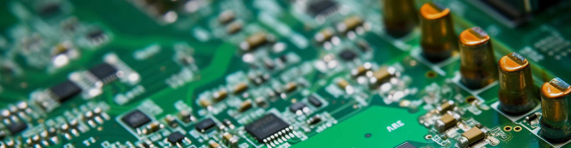
PCBA Electronic Manufacturing
PCB production and processing, SMT mounting, DIP plug-in, finished product assembly, etc
138 2887 5692 / Mr.Guo
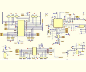
A schematic diagram is a drawing composed of electrical symbols used to analyze circuit principles. It plays an indispensable role in product debugging, maintenance, and improvement processes. Schematic reverse engineering is exactly the opposite of forward design. Forward design involves designing a schematic first, and then designing a PCB based on the schematic. PCB reverse engineering schematic refers to exporting the schematic of a product based on existing PCB files or physical PCBs, in order to facilitate technical analysis of the product and assist in later product prototype debugging, production, or improvement and upgrading.
The principle diagram of Fuwangxin Technology is developed based on the chip signal as the clue, and the pin signal names are labeled. At the same time, attention is paid to the correspondence between the packaged pins and the physical pins, the P/N polarity of the transistor and the accuracy of EBC, and strict network verification is carried out between the principle diagram and the PCB to ensure that the component position numbers, models, network names, etc. in the diagram are clear and traceable, ensuring a 100% success rate and strong readability.
According to various customer needs, Fuwangxin Technology's schematic reverse engineering service also provides reverse engineering methods applicable to multiple software, ultimately providing customers with schematic formats including PROTEL, POWER LOGIC, and layered PDF.
In addition, when conducting schematic reverse engineering for large circuits, Fuwangxin Technology abandons the commonly used practice of expressing connection relationships through bus and network labels such as net1 and net2. Instead, it first understands the circuit, then divides it into small modules based on circuit functions, and then draws them according to regional modules, adding appropriate signal signs and annotations. This solves the problem of the schematic not being intuitive and the circuit not being understood when printed, allowing the drawings to be printed on paper in a timely manner with or without the help of a computer, and the circuit to be clear and intuitive.
At present, the schematic reverse engineering services we provide mainly include:
★ High frequency board reverse drawing schematic and modification
★ Reverse design of multi-layer blind buried orifice plate schematic
★ Reverse drawing schematic of mobile phone board
★ Schematic diagram of multi-layer server computer motherboard reverse drawing
★ Reverse drawing schematic of PCB files with more than 10 layers
★ Reverse engineering of large-scale circuit schematics