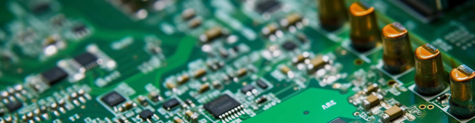
PCBA Electronic Manufacturing
PCB production and processing, SMT mounting, DIP plug-in, finished product assembly, etc
138 2887 5692 / Mr.Guo
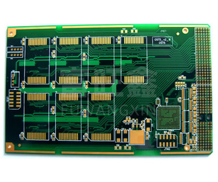
Our extensive follow-up manufacturing and processing service system has long undertaken various high-tech and high-quality mobile phone boards, double-sided, multi-layer, blind buried hole PCBs, single-sided, double-sided, multi-layer FPC and other sample making or rapid urgent sample making, which can meet customers' high-precision requirements for various PCB samples.
Professional PCB processing factories continuously improve production efficiency and economic efficiency by introducing advanced level printed circuit board production, processing, and testing equipment from countries and regions such as Germany, Japan, Hong Kong, and Taiwan. The processed product materials include epoxy glass fiber board FR4, CEM1, CEM3, BT material, thick copper foil circuit board, high TG circuit board, heat dissipation aluminum based circuit board, ultra-thin and ultra small thick gold circuit board, mobile phone battery button board, halogen-free board, Rogers high-frequency board, and high-level backplate. At the same time, it can meet various requirements of customers for sample technology, such as spraying pure tin, gold plating, immersion gold, immersion silver, immersion tin, OSP (anti-oxidation board), high TG, aluminum substrate, etc.
In terms of board production cycle, our double-sided board can be quickly processed within 24 hours, and the 4 to 8-layer board processing cycle can be delivered within 48-72 hours.
Sample process capability:
Maximum number of layers: 32 layers
Minimum line width and spacing: 3mil
Minimum laser aperture: 4mil
Minimum mechanical aperture: 8mil
Copper foil thickness: 18-175 ц m (standard: 18 ц m35 ц m70 ц m)
Peel strength: 1.25N/mm
Minimum punching aperture: Single side: 0.9mm/35mil
Minimum drilling diameter: 0.25mm/10mil
Aperture tolerance: ≤φ 0.8mm ± 0.05mm
Hole tolerance: ± 0.05mm
Copper thickness of hole wall: double-sided/multi-layer: ≥ 2um/0.8mil
Hole resistance: double-sided/multi-layer: ≤ 300 цΩ
Minimum line width: 0.127mm/5mil
Minimum spacing: 0.127mm/5mil
Surface treatment: Rosin spray tin electroplating, anti-oxidation, gold plating, carbon oil
Warping degree: ≤ 0.7%
Can meet ROHS lead-free environmental requirements, gold finger, immersion gold and other process requirements