|
2024/7/27 Sat
|
Capability
Medium and high volume
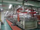
Our manufacturing facilities are located in GuangDong Province (South Of China) where high volume double sided and multi-layers conventional PCBs are produced. Currently we can support from single-layer to 16-layer with reasonable lead-time and price. Low-cost, high-quality solutions will generate our customer rapid growth and profit margins.
|
Manufacture capability
|
|
Specification
|
mass production
|
samples
|
Future
|
|
Layer Count (rigid PCB)
|
2-16
|
2-30
|
2-36
|
|
Finished Board Size(Max)
|
600 x 600mm
|
600 x 700mm
|
600 x 700mm
|
|
Finished board thickness
|
0.2 mm - 4.0 mm
|
0.2 mm - 6.0 mm
|
0.2 mm - 7.0 mm
|
|
Base Copper Weight
|
H oz to 3 oz
|
H oz to 4 oz
|
H oz to 4 oz
|
|
Finished Copper Weight
|
Up to 4 oz
|
Up to 6 oz
|
Up to 6 oz
|
|
Base Laminate Type
|
CEM-1, CEM-3, FR1, FR2, FR4, FR5(High TG)
|
CEM-1, CEM-3, FR1, FR2, FR4, FR5(High TG)
|
CEM-1, CEM-3, FR1, FR2, FR4, FR5(High TG),Rogers, Arlon
|
|
Minimum Line Width/Space
|
0.10 mm / 0.10 mm
|
0.075mm / 0.075mm
|
0.075mm / 0.075mm
|
|
Minimum Hole Size(Finished)
|
0.10 mm
|
0.10 mm
|
0.10 mm
|
|
Aspect Ratio
|
6 : 1
|
10 : 1
|
12 : 1
|
|
Surface Finishes
|
---
|
---
|
---
|
|
HASL
|
Yes
|
Yes
|
Yes
|
|
Lead free HAL
|
Yes
|
Yes
|
Yes
|
|
Immersion tin
|
Yes
|
Yes
|
Yes
|
|
Immersion silver
|
Yes
|
Yes
|
Yes
|
|
OSP(Entek or Flux)
|
Yes
|
Yes
|
Yes
|
|
Immersion gold
|
Yes
|
Yes
|
Yes
|
|
Flash gold
|
Yes
|
Yes
|
Yes
|
|
Carbon printing
|
Yes
|
Yes
|
Yes
|
|
Peelable Mask + Kapton Tape
|
Yes
|
Yes
|
Yes
|
|
Thickness of Soldermask
|
10um(min)
|
10um(min)
|
10um(min)
|
|
Cu Thickness in Holes
|
18um(min) or 25um(min)
|
18um(min) or 25um(min)
|
18um(min) or 25um(min)
|
Tin thickness
(Unit:um)
|
2~30um
|
2~30um
|
2~30um
|
Au thickness
(immersion gold)
|
0.025~0.075um
|
0.05~0.10um
|
0.05~0.10um
|
Au thickness
(Flash gold)
|
0.025~0.075um
|
0.025~0.075um
|
0.025~0.075um
|
|
Outline tolerance
|
0.10mm
|
0.10mm
|
0.075mm
|
|
Angle of G/F Chamfering
|
20,30,45
|
20,30,45
|
20,30,45
|
|
PTH, blind & buried vias
|
Yes
|
Yes
|
Yes
|
|
fire resistance
|
94V-0
|
94V-0
|
94V-0
|
|
impedance control
|
Yes
|
Yes
|
Yes
|
|
laser drilling
|
Yes
|
Yes
|
Yes
|
|
Delivery according to IPC-A-600
|
Class 2
|
Class 3
|
Class 3
|
Quick turn and samples
We fully understand that the speed of PCB services is a key element in the product life cycle. We have a quick–turn–around specialists team and special process methods for engineering, production, and logistic. Customer’s time-to-market requirements has driven us to build our service efficiently to meet the client's expectations.
|
Layer
|
Lead Time
|
|
2
|
5days
|
|
4
|
6days
|
|
6
|
7days
|
|
8
|
8days
|
|
10
|
10days
|
|